This post may contain affiliate links(s). An affiliate link means I may earn advertising/referral fees if you make a purchase through my link,
without any additional cost to you. It helps to keep this site afloat. Thank you in advance for your support. If you like what we do here, maybe buy me a
coffee.
Future Canon sensor technology - an overview
Over the past week, we’ve seen a few sensor rumors floating around, so we thought it would be a good idea to summarize what exactly Canon may bring us in the future in terms of sensors and what Canon is doing.
While the photography world hangs on Sony Electronics’ latest announcements on sensors, Canon is much quieter in terms of what they announce and what they launch.
A good example is that the only indication of dual pixel autofocus on the 70D according to rumor sites was that it was supposed to be a “new sensor”, no real details leaked out ahead of time.
Canon if anything is even tighter now than it was back when the 70D was announced making this an even more considerable challenge.
We have seen so much being mentioned on sensor technology, that we thought an overview document on various technologies, why they are important and what Canon is doing, would be good reading.
We’ve tried to keep this a generic and as non-technical as possible. If you have a high degree of technical sensor background or knowledge then this document isn’t for you.
Back Side Illuminated (BSI) Sensors
While there has been some BSI patented material, we haven’t seen much dealing with the method of manufacturing. The main expense and difficulty with BSI is flipping the unfinished sensor over and grinding the surface down to expose the photodiodes and aligning the color filter array and microlenses on the flip side using alignment marks. The alignment marks are very important, as precise alignment is critical to the process. This increases the expense of the sensor, as it’s more complicated to fabricate, and manufacturing the sensor can have greater sensors that are unusable because of errors in the manufacturing. Most of Canon’s BSI related patents seem to be around stacked sensors which we will discuss later.
BSI allows for greater wiring creativity since the wiring is unconstrained by the photodiodes.
You can see in this simplistic diagram, that the wiring layers for BSI are underneath each photodiode, instead of being around where the light enters and attempts to reach the photodiode. This path that the light travels is called a light guide. This is the main benefit of BSI, moving the wiring layers, and having the photodiode unconstrained by wiring and making light guides unnecessary.
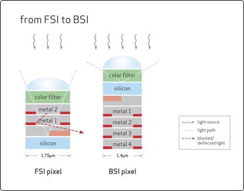
It should be noted, that BSI by itself is more important as you decrease the size of the pixel. The smartphone camera industry drove the BSI sensor development because of the ultra-small pixels in these sensors. A BSI sensor also allows for further speed improvement over a front side illuminated sensor and is important because it opens the doors to more complex sensors, such as 3D stacked sensors.
We have seen with Sony’s A7R III BSI sensor against the comparable A7R II that there’s a measurable dynamic range increase of just under 1EV at low ISO. This coincidentally is around the same difference of dynamic range between the Canon EOS R and the A7R III, as the older A7R II front side illuminated sensor is very similar to the EOS R front side illuminated sensor in terms of dynamic range.
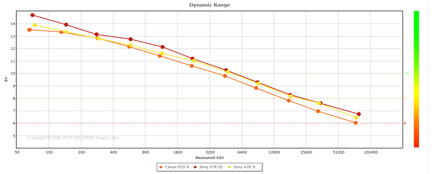
It could very well be that Canon’s sensor technology has plateaued until they go with BSI sensors
Stacked Sensors
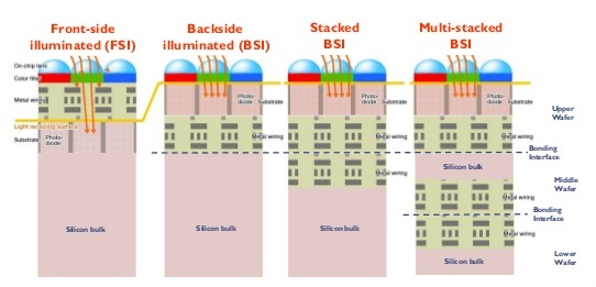
Stacked sensors are also another area that Canon has shown a great deal of research and development. We have found many stacked sensor patents over the last two years. A stacked sensor contains two or more substrates, which are individual sensor sized chips created, and then bonded together. Sony has created for the A9 as an example of a three-substrate bonded sensor (called 3D stacked). One layer for the photodiodes, the next layer for electronics, and the third for memory. Stacked sensors allow for the ultimate level of flexibility to what you contain in the sensor and can dramatically increase the performance of the sensor.
Stacked sensors aren’t inexpensive though. At worst case, you have double (or triple in the case of Sony’s A9 sensor) the actual cost of the sensor because you must create 2 or more chips of the same size as the sensor and bond them together. So while there are performance and processing gains, it’s weighted against the higher manufacturing costs. While it’s possible to use an FSI substrate in a stacked sensor, most of the technical diagrams I have seen show Canon working more towards BSI and stacked, which offers the benefit of having an easier wiring layout on the photodiode substrate. There are tricks needed though to make a stacked sensor. How the substrates communicate with each other is a hotly contested by patent material between the various manufacturers.
Here’s an example of what Sony showed for their stacked sensor design and you can see where you get the benefit of the design, as the more wiring is contained in the secondary substrates freeing up the substrate containing to the photodiodes to be just that, the photodiodes and minimal wiring. As the sensor and the stacks get more complex, a third stack can be added that contains even more electronics, or elements such as memory.
Here’s a technical drawing from one of Canon’s patents showing a stacked sensor with a BSI top layer. Given the complexity of Canon’s stacked sensor patents, we feel they are well on their way of developing stacked sensors. However, it should be noted that Canon has yet to publish a paper or show any information on stacked sensors to the general public outside of patent applications.
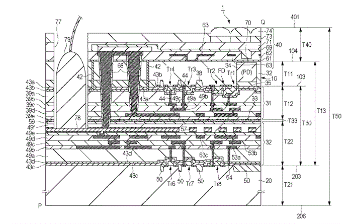
Briefly, the PD is fully exposed to the top layer with no wiring interconnects happening around the PD, this is how a BSI sensor looks. We see the wiring situated underneath the photodiodes, and the insulated bonding (shown in the picture as T33) is in between the two substrates. The wiring that connects the two substrates together is shown as item 68 in the diagram, and the external chip connection from the sensor is the big number 79 at the side of the diagram.
Stacked sensors because of the greater complexity they can achieve on the sensor also opens far more creative possibilities when it comes to global shutters. Global shutters are most likely the next big thing to hit sensors and camera technology. Global shutters will allow mirrorless to remove the last bastion of mechanical requirements to the camera – the shutter assembly. Essentially a global shutter sensor must have analog memory that stores the value of each photodiode on the sensor. With the analog memory, the values are all captured at the same instant in time and stored to memory, and then the sensor can be read the pixel values sequentially, convert them to digital values and process the image. While Canon has certainly worked on global shutter sensors, most of them are front side illuminated single-layer solutions geared towards video. Currently, Canon does have a working production sensor with global shutter. That sensor is one of the options of the C700 top-end video camera.
Quad Pixel Auto Focus Sensors
Another area of research that seems to be well developed is quad pixel autofocus sensors.
Currently, Canon uses dual-pixel autofocus sensors in most of its cameras. Essentially this means that for each actual pixel, there are two photodiodes. Quad pixel means that for each pixel there would be four photodiodes. Canon does this so that autofocus measurements can be read directly off the sensor and passed over to the lens. Each pixel can read distance. This is quite an advantage for sensor applications in mirrorless for example.
Why is quad pixel necessary? If you have ever tried a dual pixel autofocus camera in either liveview if you are using a DSLR, or on a mirrorless Canon camera such as the EOS-M50 or the EOS R, you’ll find that trying to lock focus on a horizontal line when the camera is held in landscape mode to be very difficult. This is what Quad pixel main claim to fame to be, to offer a greater accuracy of autofocus with the camera or the lines of contrast being in any direction.
Canon has also looked into other solutions for this problem, even with using dual-pixel autofocus sensors, however, it could very well be that these are far more complicated in terms of AF processing than a quad pixel sensor. For example, the following diagram shows such a dual pixel sensor, with the various pixels arranged at different angles from each other.
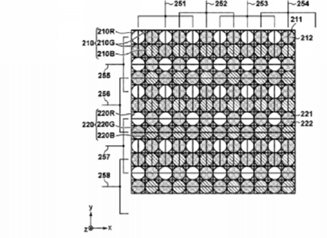
The problem with quad pixel (or even dual pixel) sensors is that the amount of data in which needs to be read for AF processing. Consider an imaginary 20MP camera; with dual pixel AF, up to 40 million data points need to be read. With quad pixel, that would double to 80 million. This would amount to 5.6 gigabits / second of data processed at 10fps. Now image a high-resolution EOS R with 70MP, that would be up to 280 million AF data points. Reading a quad pixel sensor with 70MP at 10 fps would have around 40 gigabits / second of data processed.
This massive amount of data must be processed by the camera’s processor(s) and a measurement of distance calculated so that the camera can tell the lens how much to move to achieve focus. It could be that Canon is only measuring the actual data around the AF point or region surrounding the AF point. This is possible, but I have not seen any indication of Canon doing this.
Most likely quad pixel technology will be combined with stacked sensor technology, as it can do the processing internally and massively parallel on the sensor itself.
Other technology
There are certainly other areas that Canon has explored, such as curved sensors. Curved sensors allow for greater optimization of lens optical design by curving the sensor to match the angle of incidence characteristics of the lens attached to the camera. Canon has come up with some novel ways of implementing curved sensors, but without lenses designed to take advantage of such a sensor, there would be no practical reason for the sensor to be designed that way. Where this may come into being, is on a fixed focal length compact styled camera.
In Conclusion ..
To some it seems that Canon is resting on their laurels and not doing much innovation or technology, however, we see a different picture. While Canon is not driven by business needs for advanced sensors as much as Sony Electronics who supplies a vast number of sensors to the smartphone industry, they are still working towards the lofty goals of providing advanced sensors for their cameras.
To improve their sensors will most likely have to result in more expensive methods and techniques for creating sensors for cameras. While they haven't yet done so, they are certainly researching many different means of accomplishing the goals of providing advanced sensors to their customers. Any improvement will most likely be weighed against the costs, and the sensors created when the results are favorable.

Richard CanonNews
Richard has been using Canon cameras since the 1990s, with his first being the now legendary EOS-3. Since then, Richard has continued to use Canon cameras and now focuses mostly on infrared photography. Richard is the founder and editor of CanonNews since 2017, and has worked as a writer on CanonRumors and other websites in the past.
Other posts by Richard CanonNews
blog comments powered by